

PCIe, aka PCI-Express, is a very powerful interface, and in this article, I’ll describe the basics of using it in my own projects. PCIe can be a little intimidating at first, but it’s still easy enough to experiment with and can be used as part of a hobby. At some point, you may decide to use the PCIe chip in your own projects, or use the PCIe connection on the Raspberry Pi Compute Module, for example, so it’s best to be prepared for that.
Today, PCIe can be found everywhere. Every modern computer has a number of PCIe devices that perform critical functions, and even in the iPhone, this interface is internally used to connect the processor to the flash memory and the Wi-Fi chip. We have access to all kinds of PCIe devices: Ethernet controllers, high-performance Wi-Fi cards, graphics accelerators, and all sorts of cheap NVMe drives. If you’re experimenting with a laptop or single-board and want to add a PCIe device to it, you can get a PCIe signal from one of the PCIe slots, or simply plug into an existing PCIe lane if you don’t have one. It’s been two decades since the introduction of PCIe devices, and now this technology has reached revision 5.0 and will definitely stay with us for a long time.
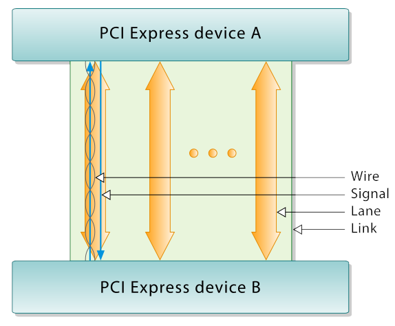
Photo V4711, CC BY SA 4.0
PCIe is tyre, which connects two devices in a point-to-point manner, as opposed to the older PCI, which could connect a chain of devices on the motherboard. On one side of this connection, there is a PCIe device, and the other side acts as a host. For example, a laptop’s CPU has several PCIe ports — one for the GPU, another for the Wi-Fi card, a third for Ethernet, and a fourth for the NVMe drive.
Each PCIe lane consists of at least three differential pairs — one representing the 100 MHz clock generator, REFCLK, which is (almost) always needed for the connection, and two forming the PCIe channel — one for transmission and one for receiving. This pattern is called the 1x line – there are also 2x, 4x, 8x, and 16x lines, which use four, eight, sixteen, and thirty-two differential pairs, respectively, plus, again, REFCLK. The wider the line, the higher its capacity.
PCIe lane width is an interesting topic with many important aspects, but first it is advisable to talk about what “differential pair” means in this context. Here at Hackaday, we’ve already Told Let’s talk about the features of differential pairs, so if you want to understand this topic more deeply, I recommend paying attention to this material. In this article, I’ll just brush up on the basics and then tell you what you need to consider when working with diffs, particularly when using them in PCIe.
▍ What’s the difference?
In simple terms, a differential pair is two opposite signals, a positive and a negative. You get the logical level of the transmitted bit by comparing these two signals to each other, instead of comparing the strength of each individual signal to the ground, as we normally do. This method is called “asymmetric signaling.” In the case of a differential pair, the signals are close to each other, and in the cables, they are even intertwined. As a result, they are affected equally by interference – since the signals for obtaining information are compared with each other, this means that the noise superimposed on both signals does not affect the final information received. Differential pairs also cause the magnetic fields of both signals to cancel each other out, which leads to a reduction in noise on the transmission line.

As a result, differential pairs allow for higher transmission rates without creating unnecessary noise or increasing susceptibility to it. For this reason, the vast majority of high-speed interfaces use this technology: Ethernet, PCIe, HDMI, DisplayPort, LVDS, and even USB, although USB2 is still pseudo-differential, but USB 3 is already complete in this sense. Fault-tolerant interfaces such as RS485 and CAN also use diffusers. Amateurs will have no trouble getting started with this technology when implementing interfaces like CAN and even USB2 — they will work over short distances no matter what, although in theory differential signals require a special approach.
However, when wiring a PCB or assembling a cable, diffs really need to be given more attention. If you don’t try hard enough in such cases, you run the risk of getting mysterious glitches or completely non-working interfaces. In this regard, I propose to analyze all the necessary requirements.
▍ Treat differential pairs with respect
First, you need to keep both diff signals side by side along their entire length. The closer they are to each other, the less exposure to external interference and the level of noise emitted by them. Given that there are often multiple differential pairs running side by side, this will also help to keep the signals of other differential pairs consistent. As for the co-laying of several differential pairs, they will need to be separated from each other and other components, whether it is polygon filling at the same level or high-frequency signals. A good practice here would be to follow “Rule 5W“, according to which there should be a distance between the center of the differential pair and the other signals equal to the width of at least five tracks. Unfortunately, it is not always possible to comply with this recommendation, but it is desirable to strive for it.
You’ll also need to make sure that there’s a continuous ground line right below these signals along the entire path of the diff pair—pouring is great. And although these two signals are compared by the receiver, each of them still behaves as asymmetric relative to the reverse current. In addition, some shielding would definitely not hurt here. If you’re connecting PCIe to a custom connector, make sure there is at least one GND pin between each pair. Finally, make sure that both tracks of the diff pair are the same length. If the diff pair rotates somewhere, one of its tracks is shortened slightly, and your PCB editor should be able to add “compensation” to this track to maintain the overall length.
Sometimes it makes sense to add multiple compensations. Photo by Phiarc, CC BY SA 4.0
There is also one nuance that is rarely spoken out — impedance matching. If you’re drawing a differential pair from point A to point B, you need to make sure you get the right impedance, and that’s easier than you might think.
Impedance is similar to resistance but refers to the change in signals. Each part of the differential path has its own impedance: the receiver and transmitter inside the chip being used, the chip pins, the PCB traces, and any connectors or cables between them if the pair is routed through them. At any point where the impedance of a signal changes, a portion of that signal is reflected from the point of mismatch, and if the change is significant enough, it will distort the resulting signal.
So, this means making sure that the PCIe lane impedance is correct along the entire path – which in practice means finding the right connectors, as well as the right track widths and spacing between them. PCIe hardware is mostly assembled with an impedance of 85 ohms. Components such as receivers, transmitters, and the corresponding connectors are out of our control, and in order to get a sufficiently uniform impedance along the entire path, we need to adjust the elements over which we have control to the same value.
For starters, if you need connectors for your PCIe lane, choose connectors that have minimal impedance mismatch. A good option would be to use high-speed models or those that are built with PCIe signals in mind – full-size PCIe, M.2, mPCIe, USB3, USB-C, and many high-speed families from different manufacturers.
Now let’s move on to adjusting the impedance of the PCB tracks. The impedance of the diff depends on many variables, but if you are a beginner electronics engineer, there are simplified calculators – Here’s my favorite. Scroll down to “Edge-Coupled Surface Microstrip”, set the track height to 35 μm and set the dielectric constant to 4.3 unless the board manufacturer recommends otherwise. Next, set the insulation thickness to the distance from the diff pairs, which can be found in the PCB documentation section for a description of the layer structure. Suppose your diff pairs are on the top layer, and the ground passes over the layer below them. In this case, look for the “prepreg” thickness between the top layer of copper and the layer below it – this value will be the height of the insulation. Next, play around with the width of the tracks and the padding between them, aiming for 85 ohm resistance. In Specifications A range of 70 to 100 ohms is allowed.
Here’s a practical exercise for you – let’s take a look at the OSHPark 4-layer board structure. Its dielectric constant (dk) is 3.6, and its minimum track width and indentation are 5 mil, i.e. 0.127 mm, or 127 μm for a calculator; The thickness of the prepreg is 202 μm. Enter the dielectric constant and prepreg thickness into the calculator and experiment with the values.

You’ll find that increasing the width of the track, pHowever, as well as reducing the indentation, it leads to a decrease in impedance – set it to the lowest possible level. You’ll see that when aiming for 85 ohms, you need to use 0.3/0.127 pairs (width/padding) – this will give 84.8 ohms. If you can’t afford this track width, then use 0.2/0.127 — this will give an impedance of 106 ohms, which is slightly out of range, but if necessary Will also work.
And finally, dilute the diffs without unnecessary maneuvers. If possible, do not run them through the holes to other layers—each pair of holes will introduce inductance into the signal, which can interfere with high-speed signals. Typically, the start and end points of a PCIe lane are on the top layer, so you should leave it that way. If you need to switch to a different layer, add grounded holes near the differential pairs. Also, keep other high-speed, fast-moving, or noisy signals as far away from them as possible. If your projects also use high-power and asymmetrical connections in addition to diffs, then install the diffs first.
So, the five important points are to lay the differential pairs close to each other, place the ground underneath them, use the proper connectors, choose the width of their tracks and indents to get the desired impedance, and also do the wiring without unnecessary maneuvers. These are all basics that need to be followed if you want differential pairs to perform their role well in the future.
▍ The Mystery of the Wet Rope
If you’ve ever worked with PCIe, you may have discovered one secret knowledge: it turns out that in practice, you don’t have to do all of the above.
You may have heard that PCIe even works on a “wet string” — the first time it’s been described that way at the 2016 World Hacker Congress, 33c3. This is a kind of hacker way to describe how PCIe works — you may not comply with many of the above points when connecting two PCIe devices, but the connection will still work. And, unsurprisingly, there’s a big kernel of truth in this – PCIe is capable of operating in suboptimal conditions, as evidenced by many examples in both the electronics and consumer worlds.
Perhaps the most accessible example is the transmission of a PCIe 1x signal using USB3, as in PCIe risers used for mining. This means that you can simply walk into a computer accessories store and buy a product that was only the result of a PCIe failure.
Another case that you may have encountered and forgotten like a bad dream is 8x PCIe Lane Routing With the help of, shudder, wires for prototyping. Thus, Toble_Miner tested the idea of creating an adapter for cheap high-speed network cards from HP servers that are incompatible with standard PCIe slots, both in pinout and mechanically. This configuration for prototyping allowed him to design a suitable version of the adapter, which we will later discuss wrote on Hackaday.
You could easily hastily run a PCIe line through an FPC cable, connecting the two cards in such a sloppy way. A similar option has been implemented in eGPU extenders using HDMI cables, and it can certainly also be implemented using a winding wire. Here link to the Linus Tech Tips experiment, in which PCIe extenders were connected in a chain that managed to reach 5 meters before the connection began to lose stability.
PCIe is a more forgiving interface compared to some others, such as USB3. It has a connection tuning mechanism – once a PCIe connection is established, the receiver and transmitter iterate over the internal parameters, adjusting them until they reach the highest possible speed with a low error rate. Further, the found parameters are used throughout the entire connection time. Also present in this interface is the retransmission of unreceived packets. In practice, PCIe is extremely stable.
Obviously, PCIe connection tuning has its own unique features – for example, for greater convenience in board design, this interface also allows you to invert any differential pair, with the exception of REFCLK, by swapping the negative and positive signals, which is detected and fully compensated for during tuning. Other technologies such as USB3, HDMI, or DisplayPort do not support such features that make the life of an engineer easier. Other interfaces often require multiple lines to have the same lengthIn addition, the data transmitted over one set of diffusers does not arrive faster than the data transmitted over the other. That being said, PCIe works great when there is a discrepancy in the length of the differential pairs, and it also detects and compensates for this discrepancy during connection tuning. And while these features are more of a facilitation of PCB design than fault tolerance, they definitely help.
▍ Strive for the best, no matter what
Dual-layer mPCIe-NVMe adapter with incorrect impedance that still works on my server 24/7
Does Such Fault Tolerance Help Electronics Engineers? Absolutely, these two features are used in virtually any professional PCIe scheme, and if you’re in less-than-ideal conditions, you can squeeze even more out of PCIe at your own risk. On the other hand, don’t neglect every rule just because someone else does—make an effort to follow these five points, even if you’re limited to a two-layer board and can’t seem to get the perfect impedance value.
Following these rules will not only teach you the discipline of using differential pairs for future projects, but it will also allow you to achieve greater signal stability, reduce errors, and delight your PCIe devices. Ignoring some or even all of these guidelines may be appropriate, as it will work in certain cases, but spending an extra thirty minutes calculating the proper impedance will help eliminate the need to design a second revision of your board and ensure that it works properly throughout its lifetime.
So here’s the general principle: Treat PCIe differential pairs with respect. If you’re using a double-layer PCB and you’re building a cheap prototype to get the result as quickly as possible, don’t just neglect impedance because you’ll have to make the tracks too wide to get 85 ohms. Open the calculator and calculate how much you can reduce the impedance value. Reducing the insulation thickness leads to lower impedance, so consider using a 0.8mm board if the mechanical design allows it. Try different component layouts to find a better path for PCIe lanes with less noise. It’s possible that tuning the connection will reduce the performance of a less-than-ideal connection by a generation or two, but it’s better than not getting a stable connection at all. Do your best to follow these rules with the resources available, and differential couples will reciprocate your respect.
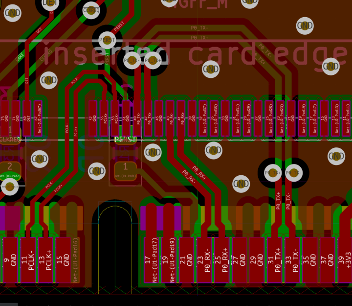
For example, if you’re using KiCad, below is a simple demonstration of how you can implement a PCIe x1 connection between two points by laying diff pairs with impedance, indentation, and via stitching.
Now you know how to route PCIe differential pairs on the board, and these tutorials will apply to all kinds of other interfaces that use differential pairs. Next time, I’ll go into more detail about PCIe signal values, line width, and bandwidth—the basics, and all the nice surprises that this interface has in store for you. If you are interested in a deeper understanding of how PCIe works, I recommend the article “The bus, that’s not a bus: the joys of hacking PCI Express” — this will be relevant if you plan to build your own PCIe devices with FPGAs.
Telegram channel with prize draws, IT news, and posts about retro games 🕹️

———-
Acknowledgment and Usage Notice
The editorial team at TechBurst Magazine acknowledges the invaluable contribution of Дмитрий Брайт the author of the original article that forms the foundation of our publication. We sincerely appreciate the author’s work. All images in this publication are sourced directly from the original article, where a reference to the author’s profile is provided as well. This publication respects the author’s rights and enhances the visibility of their original work. If there are any concerns or the author wishes to discuss this matter further, we welcome an open dialogue to address potential issues and find an amicable resolution. Feel free to contact us through the ‘Contact Us’ section; the link is available in the website footer.


![How to trick your brain and make it love challenging tasks [Дофаминовый детокс]](https://i2.wp.com/habrastorage.org/getpro/habr/upload_files/7c5/bde/804/7c5bde80498ca9b9303be21e1ac4d00e.jpeg?w=120&resize=120,86&ssl=1 "How to trick your brain and make it love challenging tasks [Дофаминовый детокс]")